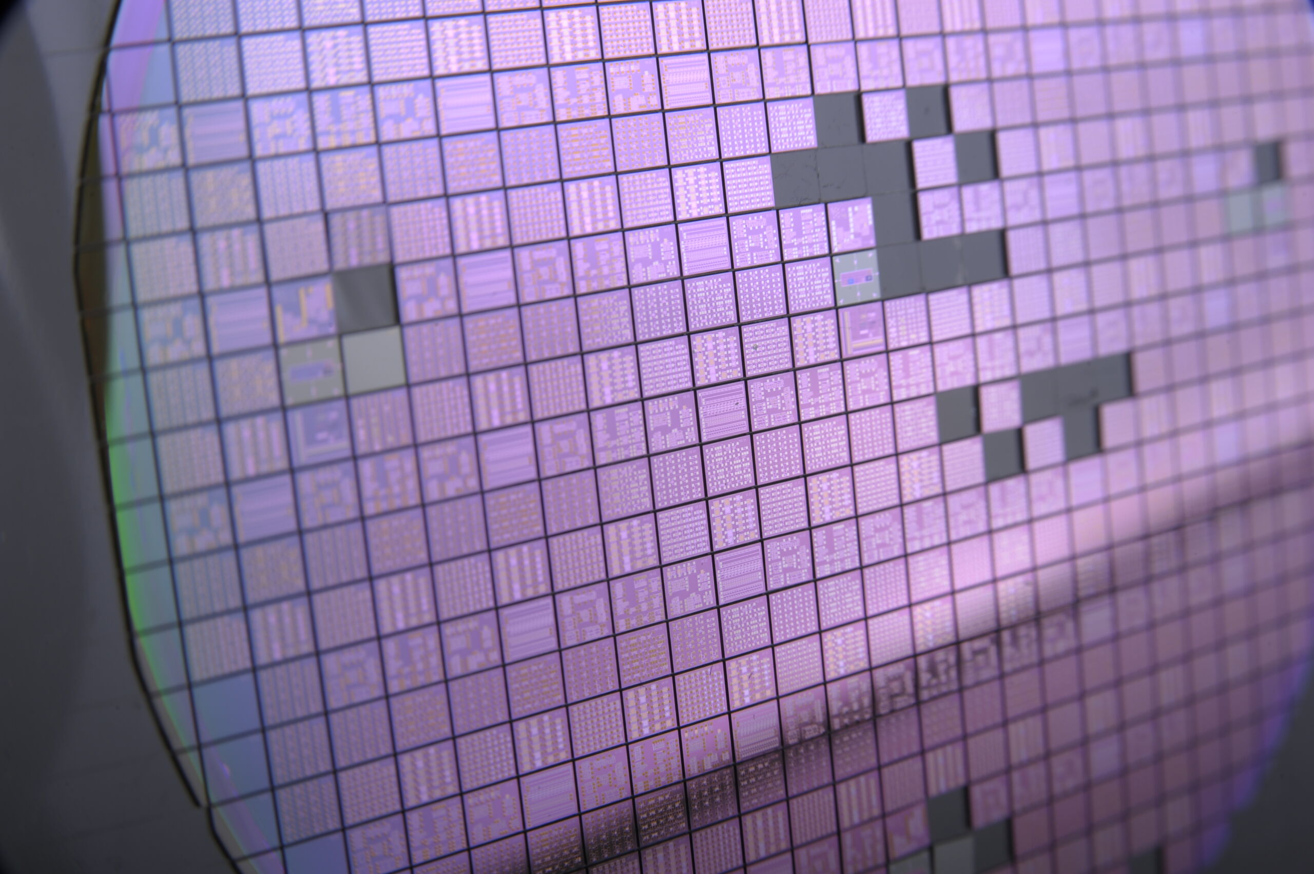
4H-SiC High Temperature
Sensors & Electronics

A technology provided by

CMOS Technology Based Sensing and Signal Processing Operable up to 600 °C

Welcome to the forefront of scientific exploration at Fraunhofer IISB, where our relentless pursuit of innovation drives us to redefine the boundaries of possibility in semiconductor technology. Dive into the intricate world of 4H-SiC High Temperature Sensors & Electronics, where every advancement opens new avenues for scientific discovery and technological breakthroughs.

We are the only provider for high temperature CMOS technology in Europe!

Technology made for harsh environments
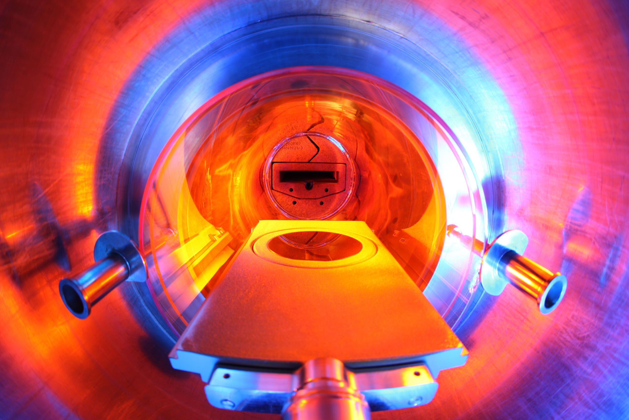
  • 4H-SiC: THE material of choice to exceed Si limits

  • 4H-SiC enabling:
  • High temperature up to 600 °C

  • Radiation hardness
  • Corrosion resistant

Technology made for harsh environments

  • 4H-SiC: THE material of choice to exceed Si limits

  • 4H-SiC enabling:
  • High temperature up to 600 °C

  • Radiation hardness
  • Corrosion resistant

CMOS-based logic and analogue circuitry
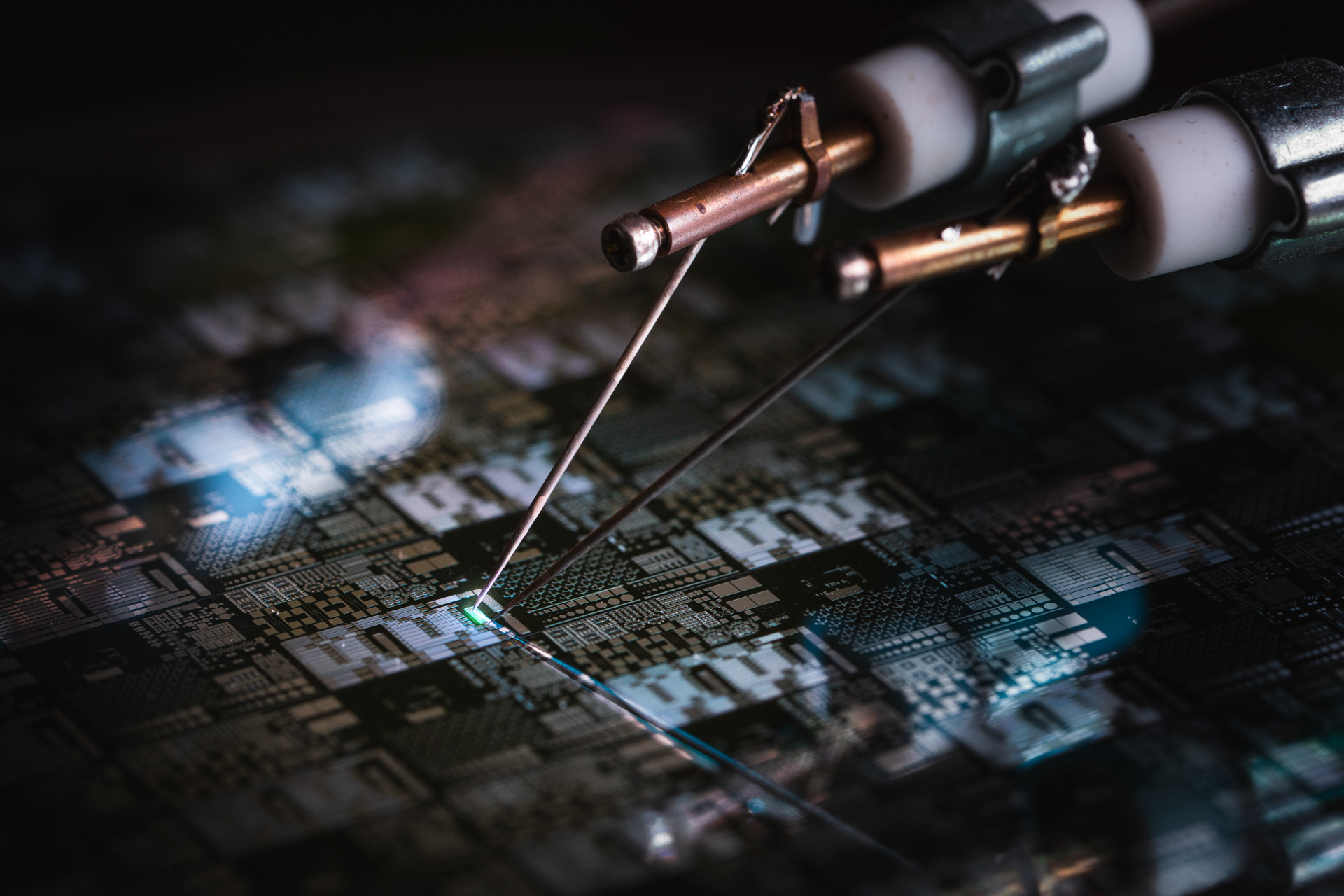
  • Lateral 2 µm prototype / early access technology

  • PDK featuring MOSFET compact models with models for passives and parasitics coming soon

  • Two metallization layers and polysilicon layer as gate electrode

CMOS-based logic and analogue circuitry

  • Lateral 2 µm prototype / early access technology

  • PDK featuring MOSFET compact models with models for passives and parasitics coming soon

  • Two metallization layers and polysilicon layer as gate electrode

Integration of sensors and power devices
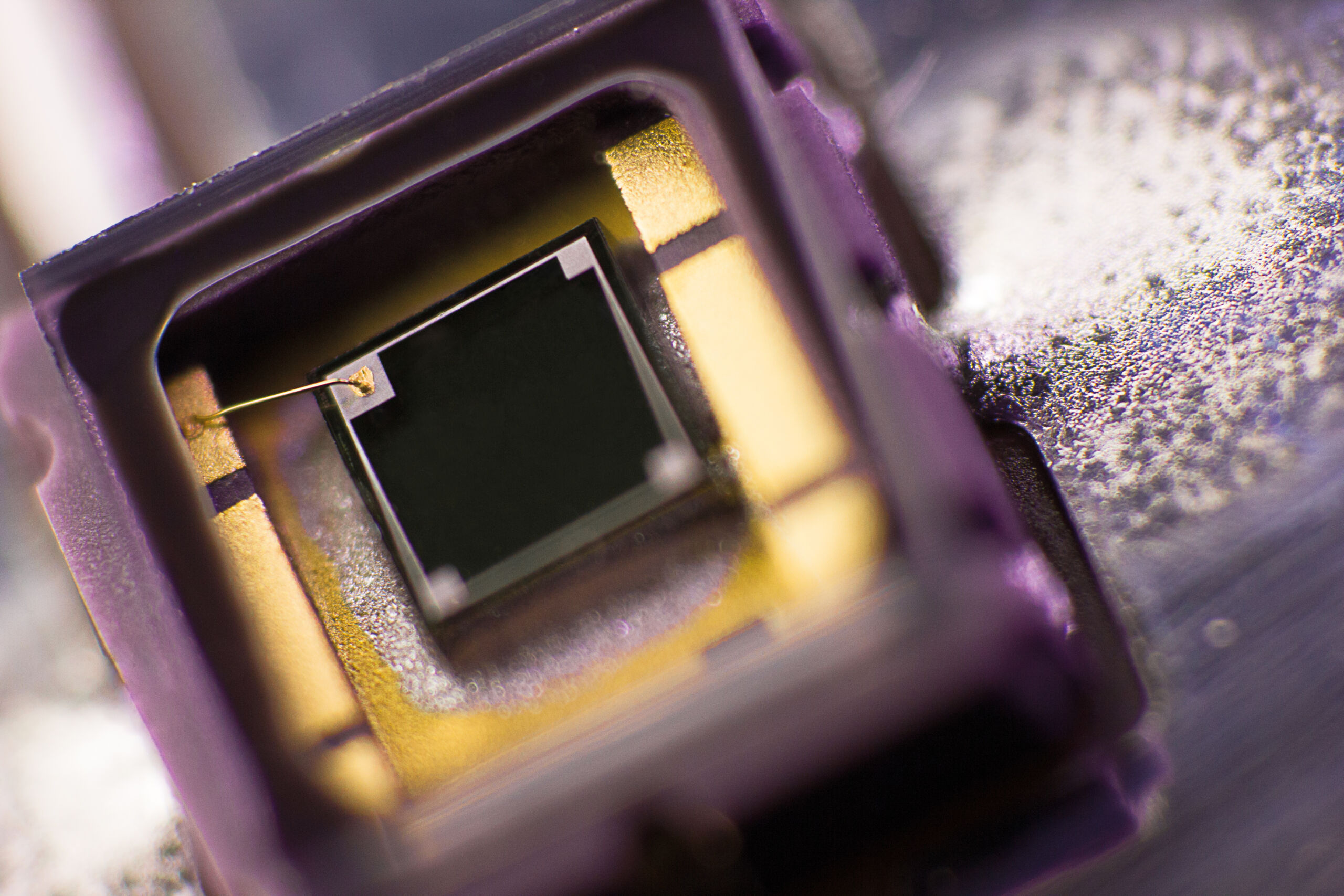
  • Smart integration for signal processing, gate drivers and more

  • Sensing solutions for temperature, UV and magnetic fields

  • Pressure sensing in development

  • Lateral power MOSFETs available
  • Options for vertical device integration

Integration of sensors and power devices

  • Smart integration for signal processing, gate drivers and more

  • Sensing solutions for temperature, UV and magnetic fields

  • Pressure sensing in development

  • Lateral power MOSFETs available
  • Options for vertical device integration

Easy access with customizable process solutions

  • Bilateral collaboration for tailored solutions from research to full wafer processing as service

  • Easy access through multi-project wafer (MPW) via EUROPRACTICE

Easy access with customizable process solutions

  • Bilateral collaboration for tailored solutions from research to full wafer processing as service

  • Easy access through multi-project wafer (MPW) via EUROPRACTICE

The entire value chain in SiC

Join Us in the Pursuit of Scientific Excellence

Collaborate with Fraunhofer IISB to embark on a transformative journey at the intersection of science and technology.
Use the contact form on the right to contact Mathias Rommel, Group Manager for SiC CMOS
Circuit Design and Characterization, and together, let us push the boundaries of scientific exploration.